How to Design an FPGA Device Protection Network
Designs based on digital signal processors (DSPs) are particularly vulnerable if the DSP does not have adequate security capabilities. In many applications, advanced security features can be easily implemented if an FPGA is used in coordination to offload some of the DSP’s work. Moreover, if the cooperating FPGA uses flash storage technology, the configuration bit stream and key key information in the structure are stored on the chip, which can achieve inherent security against copying or cloning, enabling designers to automatically protect the design from these type of theft.

DSP and FPGA System Architecture
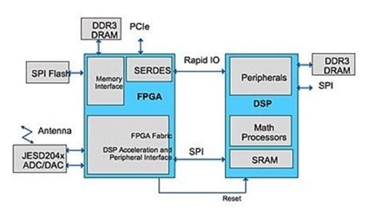
In a system using an FPGA or DSP (Figure 1), the DSP implements advanced signal processing algorithms and the FPGA implements the front-end decimation. A high-speed serial RapidIO bus is used to connect the FPGA and DSP; the FPGA is also connected to the PCIe bus and is used as a remote access management port via the Internet.
The PCIe bus can also bridge traffic into and out of the RapidIO bus, with a view to connecting extended remote management to the DSP. The FPGA controls an external DDR3 DRAM, which serves as a buffer for packets sent and received over the wireless interface, and allows the FPGA to offload any low-level data protocol processing and buffer management functions from the DSP.

The FPGA will also be responsible for “booting” the DSP from the external SPI Flash. The FPGA uses its own SPI memory as the source of the DSP code to map the boot process through the boot function from the DSP’s SPI port. Once the code transfer is complete, the FPGA allows the DSP to begin execution.
Secure Root
If the system does not protect the boot process, an intruder can replace it with their own code and then effectively hijack the entire system, which can result in damage to the system, significant financial loss, and possible personal liability. We must use a secure boot process to minimize such attacks, and a hardware root of trust is necessary to implement a secure boot process.
A hardware root of trust supports the verification of system data integrity and confidentiality, while extending this trust to internal and external entities. A hardware root of trust protects against hacking or modification, and can also serve as a starting point for securely laying out more advanced features. In embedded systems, the Root of Trust works with other system components to ensure that the main processor boots securely using only authorized codes, thereby extending the domain of trust to the processor and its applications.
The hardware Root of Trust must be built on a secure FPGA, and its configuration bitstream must be protected from copying or reverse engineering to prevent the Root of Trust from being compromised by malicious intruders. Therefore, protecting the intellectual property (IP) of the FPGA device is necessary to protect the rest of the embedded system.
Safety Requirements for Multi-Stage Boot Processes
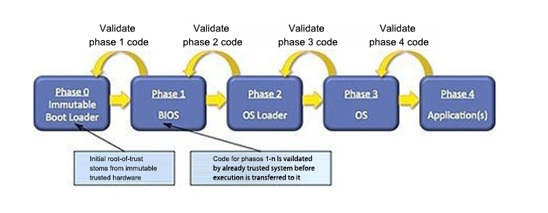
Initialization of the embedded processing system from other parts requires a secure boot process to execute trusted code that is not affected by malicious content or leaks. Figure 2 shows the various stages that a secure boot process must go through to adequately protect the initialization of an embedded system. Each stage must be verified by the previous successful stage to ensure a “chain-of-trust” up to the top application layer.
The unmodifiable bootloader (stage 0) code can be embedded in the FPGA device and verified through a secure root of trust using protected security keys and associated security algorithms to ensure code integrity and authenticity. Before transferring code and execution to the sequential stages of each secure boot, these stages must be verified by a previously trusted system.

Implementing secure embedded systems
Encrypting the bitstream data is a common method of protecting the configuration bitstream used for power-up, as it is for SRAM-based FPGAs. This makes it more difficult to capture the bitstream just by observation during configuration startup. The decryption key is stored in the FPGA and is used to decrypt data before configuring the FPGA. Batteries are usually required to retain security keys in the event of a power loss.
Another way to protect the FPGA configuration bitstream is to use non-volatile memory to store it entirely on-chip, avoiding exposure during startup. Some FPGA devices, such as Microsemi’s SmartFusion2 and IGLOO2 families, also provide additional protection by encrypting the bitstream when programmed during manufacturing. This also protects the design from duplication or reverse engineering by unscrupulous contract manufacturers, which would compromise the required hardware root of trust.
Once we have created a secure FPGA, the next major requirement is to implement a hardware root of trust. The FPGA must protect the security key and the on-chip immutable initial stage (Phase 0) bootloader, making them completely impossible to attack or modify by malicious intruders.
If a Flash-based FPGA is used to store immutable code and security keys on-chip, the configuration bitstream can also be loaded via the configuration process for security. The security key is only a small part of the overall design, however, it is very important to protect the design from other forms of attack.
Haoxinshengic is a pprofessional FPGA and IC chip supplier in China. We have more than 15 years in this field。 If you need chips or other electronic components and other products, please contact us in time. We have an ultra-high cost performance spot chip supply and look forward to cooperating with you.
If you want to know more about FPGA or want to purchase related chip products, please contact our senior technical experts, we will answer relevant questions for you as soon as possible
Our Products