Authoritative Guide to FPGA System Integration
FPGAs are complex devices and are being used in an increasing number of systems. The complexity of FPGAs is both an advantage and a disadvantage. The reason for the advantage is that they bring many system performance benefits and capabilities to the designer. The reason for the disadvantage is because of the complexity of successfully integrating a high pin count FPGA into a high speed system. Many things can go wrong – including pin assignments that don’t work in the board layout, signal integrity issues on the board, power and ground issues, parasitic package inductance, and more. This article focuses on some of the challenges and system integration issues that need to be faced when using FPGAs, including printed circuit board (PCB) design, software debugging, and power management.

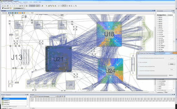
It is not uncommon for an FPGA to go through four or more design iterations before reaching the “final” I/O pinout. One of the challenges for FPGA users can be waiting for the actual “final” pin assignments; many performance factors can arise during system integration that can require a redesign of the FPGA layout.
Considering that about one-third of designs contain multiple FPGAs, the challenges can be multiplied. PCBs used in FPGA-based systems are complex and sophisticated interconnect systems. Co-design, communication, and collaboration between FPGA developers and PCB designers can prevent many potentially catastrophic changes to the physical design of the PCB as the FPGA goes through multiple iterations.

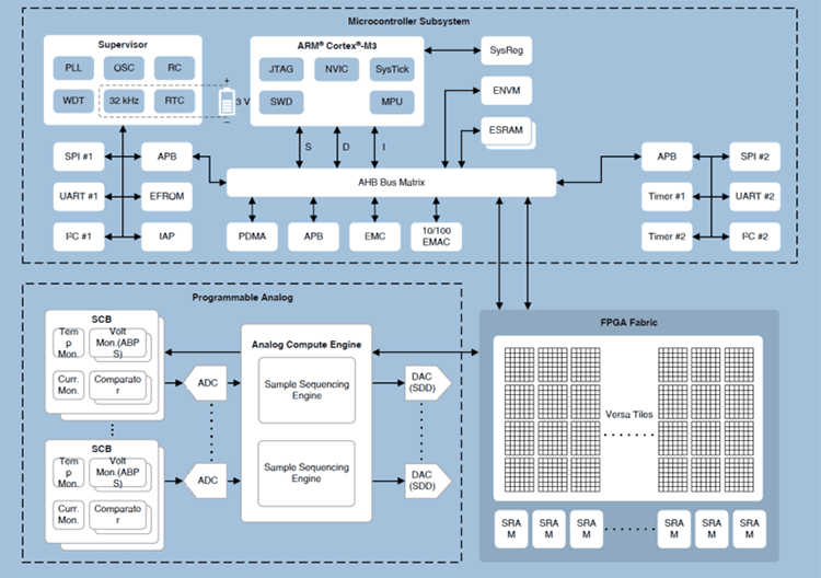
The greater flexibility of FPGAs compared to ASIC- or CPU-based designs can be important. Various architectural approaches can be created and tested until the optimal design is achieved. FPGAs with on-chip processors offer a trade-off between CPU-based discrete processing and FPGA-based embedded acceleration capabilities. If implemented properly, it can reduce the time required to design, test, and validate new designs.
FPGAs support hardware and software cores for standard functions such as various communication buses, which can simplify the testing required for these standard functions. The FPGA can also include an on-chip ARM processor. Existing processor code can be ported into the design and new code created in parallel with the system design.
When integrating standard processors and standard interface buses, FPGA users have access to numerous code libraries, drivers, functional APIs, RTOS, and more. This speeds up the development process and enables the use of standard simulation and testing solutions, further accelerating development time. Finally, the FPGA itself can help manage debugging because it contains additional hardware capabilities specific to this activity.
Debugging Issues with FPGA Designs
Due to the complex and extensive functionality of FPGAs, the time to debug a new design can account for 50% or more of the total design time. System-level timing issues can be a serious challenge. FPGAs often have multiple timing domains, and a common source of problems is asynchronous errors, especially across timing domains. These can be particularly challenging and often only arise when a specific set of circumstances (such as a specific data pattern) exists.
Interference between multiple power rails and low signal fidelity between adjacent ICs can also be the cause of timing issues. Crosstalk, reflections, general signal noise, and EMI can all cause timing violations. Properly manufactured PCBs can suffer from various disturbances due to power-related issues such as voltage transients, load surges, and excessive power dissipation.

Like high-performance systems in general, FPGA-based systems are increasingly complex and require additional passive components, such as resistive terminations and decoupling capacitors, to help with noise and signal issues. Embedded passives can be found on more and more inner layers of PCBs as they reduce interconnect size, board area and provide superior performance.
The I/O groups on the FPGA are dedicated to multi-gigabit communications. Achieving clean data transfer at these speeds requires precise implementation of PCB interconnects and careful matching and control of the driver and receiver operating characteristics. At multi-GHz frequencies, even small vias can look and behave like antennas, degrading signal quality. For example, the PCI Express bus specification strongly recommends using more than two vias per trace and matching trace lengths to within a 0.025% tolerance.
Co-design, communication, and collaboration between FPGA developers and PCB designers can also address the complexities of powering FPGAs. The flexibility of FPGAs allows designers to assign different voltages, drive strengths, and slew rates to different pins. Ringing and crosstalk may be introduced on the PCB if FPGA vendor specifications and guidelines are not followed. Additionally, the power supply can introduce random switching noise that can cause jitter or variation in bit transition timing relative to the data rate clock.
Power Issues and Challenges
Power requirements in FPGA data sheets are becoming more complex and more important. Large FPGAs can have more than 12 power rails, some of which require 40-50A of current. FPGA power system design considerations include:
- Current requirements for a single power rail
- Sequence various voltage rails
- Various voltages rise monotonically
- High voltage accuracy
- fast transient response
Common FPGA powering solutions include the use of distributed power architectures, where a relatively high intermediate bus voltage (such as 48Vdc or 12Vdc) is supplied to the FPGA area, followed by various non-isolated point-of-load (PoL) dc/dc converters. This is especially useful for providing high current rails. In addition, power management ICs (PMICs) that contain multiple DC/DC converters on a single chip can be used. In practice, it is common to use a mix of discrete PoLs and one or more PMICs.
FPGAs require a range of voltage rails from below 1V to as high as 3.3V, and sometimes even higher. Examples of voltage requirements include: If a particular bank has DDR2 SDRAM attached, a 1.8V driver and 0.9V reference is required; if an LVDS bus is attached to the bank, a 2.5V power bus is required instead of 1.8V; and, although DIMMs typically require 1.8V V SSTL signal, but various types of I2C signals may require different voltages.

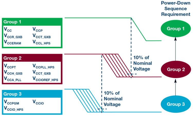
FPGAs often require that various voltage rails be powered up and down in a specific order. To prevent damage, the core voltage is usually specified to power up before the I/O voltage, while some auxiliary functions may require power up after the I/O voltage. In addition to sequencing, the various voltage rails also need to rise monotonically during startup. This requires that the voltages only rise during startup; they cannot rise, fall, and rise again for a period of time.
Additional power controller ICs may be required. PMBus are commonly used to control various DC/DC converters. These power management ICs can also integrate extensive digital monitoring and power system management, including protection circuits for thermal and overcurrent, short-circuit and UVLO faults.
At the end of the startup period, the various voltages are subject to strict regulation and accuracy requirements. FPGAs can be powered on and off quickly and consume high current at startup. Therefore, they require extensive voltage decoupling for high current inputs. Ceramic capacitors up to 1mF can typically be found on the input pins. Designers should carefully check the maximum output capacitance specified for the various switching regulators and LDOs used in FPGA designs. Too much capacitance can degrade power converter performance.
Choosing the correct capacitor for the input pin also affects voltage accuracy. 3% voltage accuracy is common in FPGA power supply specifications. Various types of ceramic capacitors may have widely varying values under changing operating conditions. It is important to use capacitors that are stable enough under the expected operating conditions.
Integrating an FPGA into a system requires dealing with many challenges, including pin assignments that don’t work in board layout, signal integrity issues on the board, power and ground issues, parasitic package inductance, and more. This article addresses some of the challenges and system integration issues faced when using FPGAs, including PCB design, software debugging, and power management.
Haoxinsheng is a professional supplier of FPGA, electronic components, chips and other products. Our products have a wide range, affordable prices, and comprehensive after-sales services. The products on sale include INTEL, AMD, XILINX, ALTERA, MICROCHIP and other brands. If you have more needs, please contact our senior technical engineers, and we will reply to your questions as soon as possible.