Basic structure and default state of FPGA IO
When designing FPGA hardware, pin assignment is a very important part, especially the pins that need to communicate with other chips on the hardware circuit. The state of pins of Xilinx FPGA at various stages during the whole process from power-on to normal operation will have a very important impact on hardware design and pin assignment. Today, we will analyze the status of all IOs in the whole process of FPGA from power-on, configuration program, to normal operation.

The time phase can be divided into two parts, the first phase is from the FPGA power-on until the configuration is completed. The second stage is that after the configuration is completed, the FPGA starts to work normally.
In terms of pin types, it can be divided into three categories: the first category is ordinary IO, which is further divided into IO used in programming and IO not used in programming (that is, there is no IO in ucf or XDC file). Constrained IO); the second type is dedicated download configuration pins (Dedicated Pins), which are only used for dedicated functions, including M[2:0], TCK, TMS, PROGRAM_B, INIT_B, etc. The third type is function multiplexing pins, which are used when using specific functions. For example, when using BPI configuration mode, D[00-31] and A[00-28] need to be used. If using SYSMON, I2C_SDA and I2C_SCL need to be used. However, when this function is not currently used, the function multiplexing pin can be regarded as a common IO.
Basic structure of FPGA IO
In “Various Modes of IO Input and Output”, the various input and output modes and principles of processor IO are introduced, so what is the structure and principle of FPGA’s IO? Figure 1 shows the internal structure of the IOB provided in the Xilinx documentation. It can be seen that:
Inside the FPGA IOB, before the Pad output, there are built-in pull-up and pull-down resistors. And can control whether the two MOS tubes are turned on or not through the Passive Pull-up/Pull-down module to control whether to enable the pull-up and pull-down resistors.
There are an Input Buffer and an Output Buffer for the internal connection to the Pad. The Input Buffer should always be in a high-impedance state to the outside world, and at the same time, the level on the Pad can be passed to I1 and I2 through the Input Buffer, or the lower FF. The Output Buffer has two control signals, namely Slew Rate Control, which is used to control the Slew Rate of the output signal; the other is the tri-state control signal T, which can control the Output Buffer to output high impedance.
The internal output signal Out can be output through the FF in the upper part after being synchronized by the Output Clock, or it can be directly connected to the input of the Output buffer for direct output.
Similarly, the output of the Input Buffer can be directly connected to I1 and I2, or it can be output to the internal bus after the synchronization of the input clock through the FF in the lower half.
The upper and lower MOS tubes are not push-pull output MOS tubes, because they are not controlled by complementary signals, so one is not necessarily turned on and the other is closed.

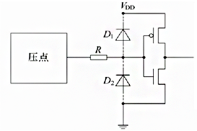
The structure and principle of the input buffer are introduced here. The structure is shown in Figure 2. Its principle is very similar to that of the push-pull output circuit, except that the input signal is used as the control end of the two complementary MOS tubes, which controls the level of the output end. . Since the input buffer has its own supply voltage, the input level must match the supply voltage of the buffer. The two clamping diodes D1 and D2 are used to prevent the input voltage from being too low or too high and damaging the input buffer.

Ordinary IO
Before the FPGA is powered on until the configuration is completed, because the current FPGA has not downloaded the program, it is impossible to distinguish which pins are used by the design and which pins are not used. The ordinary IO at this time includes two parts:
All general purpose IO pins in this package.
All function reuse pins that are not used in the currently selected mode.
In the Spartan6 family and earlier devices the state of these pins is based on the state of HSWAPEN.

In 7 series and later devices, including Ultrascale devices, the state of these pins is based on the PUDC_B (Pull-Up During Configuration) pin

The functions of these two pins are similar, and they are both used to control whether the pull-up resistors of all common IOs are enabled before the Configuration is completed. Corresponding to Figure 1, that is, the Output Buffer outputs high impedance, and the Input Buffer is always high impedance externally. At this time, choose whether to connect the pull-up resistor.
After the configuration is complete, the FPGA enters the normal working mode. After the configuration is completed, the common pins can be divided into the following two types:
IO used in engineering design, that is, IO with explicit constraints in UCF or XDC.
The rest are not used and have no bound IO. (called Unassigned Pins)
First of all, for the first case, since the settings of these pins have been clearly set in the design, including direction, level, drive capability, etc., after the configuration is completed, the state of these pins has been set to the preset set status.
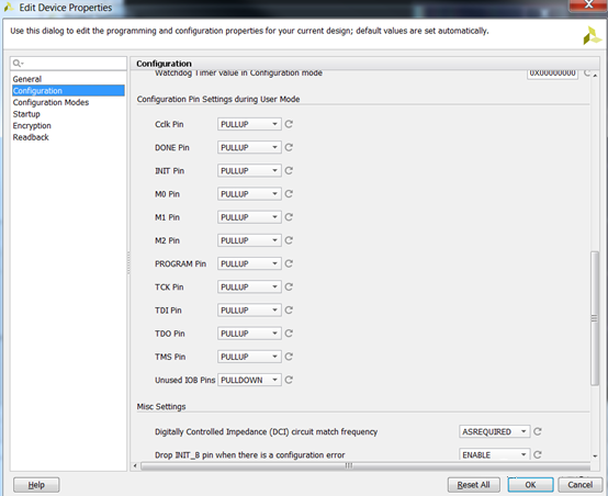
For unconstrained IO, it’s a bit more complicated. In the ISE development environment, after the project is implemented, there is a “-g UnusedPin Unused IOB Pins” property in Processà Process properties àConfiguration Options, you can choose Pull Down, Pull Up or Floating. The default state is Pull-Down. Corresponding to Figure 1, it is a high-impedance output that turns on the pull-down resistor. The other two settings are high-impedance plus pull-up resistors or just the pull-up and pull-down resistors are not conducting.
There are the same settings in Vivado. After the implementation is completed, open the Implementation Design and select bitstream Settings. In the Configuration column of “Configure additional bitstream settings”, there are the following property options.

Dedicated IO
All dedicated configuration pins are located in Bank0, including CFGBVS, M[2:0], TCK, TMS, TDI, TDO, PRORAM_B, INIT_B, DONE, and CCLK. The meaning of dedicated pins is that these pins are only used for configuration at any stage during or after configuration.
Therefore, it is relatively simple to consider these pins, which are divided into input signals and output signals. The state of the input signal always maintains the LVCMOS level standard, and the voltage value is VCCO (why does the input signal also have a level standard requirement, it needs to match the power supply voltage of the Input buffer, see Figure 2). The state of the output signal always maintains the LVCMOS level standard, the voltage is VCCO, 12mA drive, fast slew rate.
Function multiplexing IO
Compared with other pins, the situation of function multiplexing pins is the most complicated. These pins include configuration-related PUDC_B, EMCCLK, CSI_B, CSO_B, DOUT, RDWR_B, D00_MOSI, D01_DIN, D[00-31], A[00-28], FCS_B, FOE_B, FEW_B, ADV_B, RS0 and RS1; and ADOP to AD15P, AD0N to AD15N, I2C_SDA and I2C_SCLK related to System Monitor.
In order to clarify the status of the function multiplexed pins at different stages, the multiplexed pins are divided into the following categories:
Function multiplexing pins used in the currently selected function, such as D[00-31] and A[00-28] when BPI configuration is selected.
Function multiplexing pins that are not used in the currently selected function. For example D[00-31] and A[00-28] when SPI configuration is selected.
Before completing the configuration, it needs to be used as an output or bidirectional. In short, it is possible to output a signal to the outside, such as I2C_SDA and I2C_SCLK.
During the period from the power-on of the FPGA to the completion of the configuration, the first type of pins listed above, that is, the function multiplexing pins used in the currently selected function, are equivalent to the dedicated configuration IO pins. The state of the input signal always maintains the LVCMOS level standard, and the voltage value is VCCO. The state of the output signal always maintains the LVCMOS level standard, the voltage is VCCO, 12mA drive, fast slew rate.
The second type of pins listed above, that is, the function multiplexing pins that are not used in the currently selected function, are regarded as ordinary IO, and their status is controlled by the HSWAPEN or PUDC_B signal, which determines whether it is high-impedance or connection. Weak pull-up resistors.
The situation of the third type of pins is more complicated. At present, only I2C_SDA and I2C_SCLK are known. These two signals will have some uncertain states before the configuration is completed. So if the IO of the FPGA is still spare, and all the pins connected to the outside are required to have a certain state, then it is best not to use these two pins as the IO for connecting peripherals.
After the FPGA configuration is complete, the three aforementioned pins are divided into three other categories:
The first type is that the function pins that need to be reserved are clearly configured in the user design. For example, the Persist option attribute is set for the configuration-related pins. In this case, these pins will continue to maintain the previous configuration-related functions and their states. The state of the input signal always maintains the LVCMOS level standard, and the voltage value is VCCO. The state of the output signal always maintains the LVCMOS level standard, the voltage is VCCO, 12mA drive, slow slew rate. For another example, SYSMON is used in the design, and the I2C_SDA and I2C_SCLK pins continue to maintain the function of DRP I2C.
The second type is that there is no requirement to retain their special functions in the user design configuration. These pins will become ordinary IOs after the configuration is completed, and IOs that are not used in the user design. These IOs are equivalent to Unassigned IOs. As mentioned above, the status of these IOs after configuration is affected by the corresponding settings, which can be pull-up, pull-down or Floating.
The third category is that there is no requirement to retain their special functions in the user design configuration. These pins will become common IOs after the configuration is completed, and the IOs used in the user design. The state of these IOs is controlled by the user design and will be set in XDC or UCF. If it is not set, it will follow the default state. The default state of the input port is the LVCMOS level standard, and the voltage value is VCCO; the default state of the output signal is to maintain the LVCMOS level standard, the voltage is VCCO, 12mA drive, and slow slew rate.
Haoxinshengic is a pprofessional FPGA and IC chip supplier in China. We have more than 15 years in this field。 If you need chips or other electronic components and other products, please contact us in time. We have an ultra-high cost performance spot chip supply and look forward to cooperating with you.
If you want to know more about FPGA or want to purchase related chip products, please contact our senior technical experts, we will answer relevant questions for you as soon as possible
Our Products