Common open test applications based on FPGA
Most instruments today implement the various functions of the instrument by combining an enclosed FPGA with fixed firmware. If you’ve seen a disassembled scope, you’ve probably seen the FPGA inside. The FPGA increases the processing power of the test instrument, and if you can use the open FPGA in the instrument, you can write the test functions of the instrument yourself.

Instrument manufacturers have long recognized the benefits of FPGAs and have used their unique processing power to implement various instrument features:
- Pre-trigger acquisition on oscilloscope
- Generate I and Q data through signal processing on a vector signal analyzer
- Real-time implementation of pattern generation and vector comparison of high-speed digital instruments
Test equipment manufacturers are working to help users make better use of FPGAs to optimize for more specific applications. To help you understand the benefits of this shift, the following are key attributes of FPGAs that are particularly well suited for test applications
-
Determine real-time processing
-
True parallel execution
-
Reconfigurable
-
Low latency
Thinking a little bit further, what can you do with an open FPGA that wasn’t possible before? To illustrate these possibilities, here are some common test applications that utilize open FPGAs
1. Accelerated Test System
In end-of-line production testing of high-volume production lines, test time counts against the clock. Production efficiency is maximized when the test rate of the production line is matched to the production rate. If this match cannot be achieved, innovative techniques must be employed to reduce test time.
The traditional method is to connect a stand-alone benchtop instrument to a host PC via Ethernet, USB or GPIB. Since the device under test is controlled, measured and processed through different data buses, the required test time is relatively long. Another approach is to use an open FPGA to accelerate the process, as shown in Figure 1.
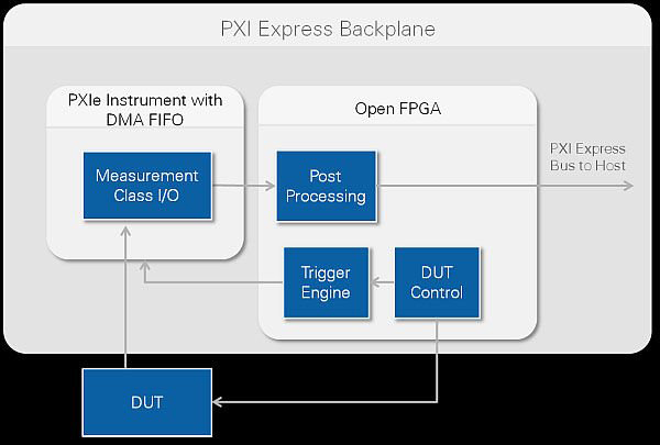
Figure 1: In a test instrument, an open FPGA enables functions such as triggering and post-processing.
Instead of utilizing an external communication bus, an FPGA uses a high-speed bus such as PXIe to connect instruments and connect to the device under test through its configuration ports such as I2C, SPI, or other control buses. In such applications, the FPGA can control the DUT (device under test), trigger other instruments to start collecting sampled data, and even process the sampled data to convert it into a meaningful result for the host.
Low latency is a key factor in enabling such applications to run faster. The FPGA itself does not have an operating system, it implements all logic on hardware with high clock rates. This means that a response may take one clock cycle to acquire, one clock cycle to process, and one clock cycle to respond.
If the clock rate is 200MHz (clock period is 4ns), a complete response takes 12ns. Due to the deterministic nature of FPGAs, this response is not one-time, but 12ns each time. As a result, the FPGA can eliminate host-related delays and minimize the non-deterministic delays of host-based processing.
2. Protocol aware
Today, not all digital and MEMS devices can be tested against known result vectors. For example, give a PDM (pulse density microphone) an excitation signal, due to the analog nature of the PDM, the bit stream obtained from each test will be different. In order to obtain meaningful results related to such a device under test, the digital stream needs to be decoded according to the corresponding protocol first, and then the results can be compared.
With an open FPGA, you can configure your test system to execute the PDM protocol on the FPGA instead of transferring it to the CPU for interpretation. In a broader sense, you can configure an FPGA today to perform a PDM protocol, and tomorrow the same FPGA can be reconfigured to perform other protocols to test digital temperature sensors, accelerometers, or MEMS devices.
In Figure 2, the protocol is not executed on the CPU, but on the FPGA. Because of this, the test system can support fast handshake scripts, accommodate protocol behaviors such as precise wait periods, and make decisions based on this communication. Not only does this approach allow you to receive higher-level data from the DUT, such as analog data decoded by a PDM microphone, but it also allows you to use higher-level commands to write test scripts.
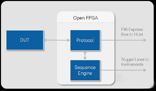
Figure 1: In a test instrument, an open FPGA enables functions such as triggering and post-processing.
3. Closed Loop Testing: Power Amplifiers
In a wireless communication system, a power amplifier integrated circuit can increase the strength of a signal before sending it to an antenna. A power amplifier usually has a specific performance at a specific output power. Therefore, it is necessary to test the power amplifier when it is operating at a specific output power level.
However, we usually only know roughly the gain of the amplifier (eg ±3dB), and the gain of the amplifier is nonlinear over the operating range of the device. The closer to the maximum output power, the lower the gain. Therefore, the output of the amplifier must be “tuned” before any performance measurements can be made. Output trim is often referred to as power trim or power servo. The basic principle is to adjust the input power of the amplifier until the correct output power is measured.
A conventional test setup for measuring power amplifiers is shown in Figure 3. The VSG (Vector Signal Generator) generates a stimulus waveform to the DUT (Device Under Test). A power meter ensures that the DUT is outputting the correct power level. Finally, a VSA (Vector Signal Analyzer) measures the performance of the device under test – such as EVM (Error Vector Magnitude) or ACP (Adjacent Channel Power). These measurements were made at various center frequencies and power levels.
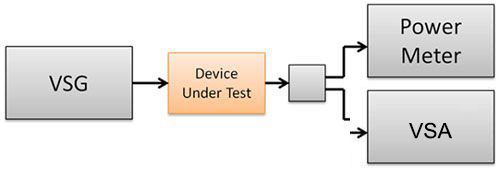
The output power of the power amplifier must be adjusted for each desired center frequency and power level. The following steps can be followed during the adjustment process:
- Choose a starting VSG power level based on the estimated gain of the device under test.
- Set the VSG power level.
- Wait for VSG to stabilize
- Wait for the DUT to stabilize
- Use a power meter to measure.
- Exit if power is within range. Otherwise calculate the new VSG power level and return to step 2
The time required for adjustment depends on the type of device under test, the desired accuracy, and the type of instrument used, and is typically a few hundred milliseconds to a few seconds. After tuning is complete, use VSA for performance measurements.
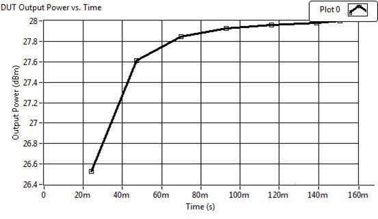
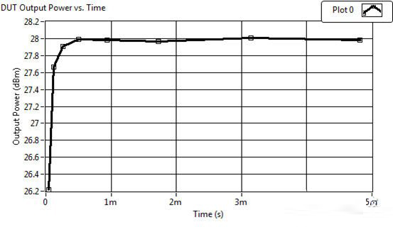
Figure 4 shows the output of a device under test during adjustment using the traditional method to achieve an average output power of 28dBm. If the gain of the power amplifier is linear and matches the standard gain specified in the datasheet, the first point generated by the VSG will output 28dBm.
On the contrary, the output of the amplifier is only 26.5dBm, which shows that the standard gain specified by the power amplifier is not accurate. Therefore, the VSG output power needs to be adjusted while the VSA captures another point. The average power at this point is 27.6dBm, which indicates that the amplifier is in gain compression.
Overall, the method requires seven steps and about 150 milliseconds to bring the amplifier’s output to the desired level. In this example, the DUT settling time for each step is 10ms. However, the settling time varies for each device under test, which greatly affects the overall settling time.
VST (Vector Signal Transceiver) combines VSG, VSA and FPGA. This combination allows you to offload the operation of the power scaling algorithm to hardware. In Figure 5, although there is no power meter, you can also run a system calibration step to get the same accuracy on the VSA as the power meter.
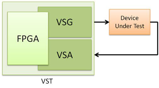
The output power adjustment steps of the power amplifier are similar to the traditional method steps, except that the adjustment loop is run inside the open FPGA. Running the loop inside the FPGA greatly reduces the time required for each adjustment.
By using an open FPGA and executing the control loop on the FPGA, the time required to adjust the DUT output power is significantly reduced compared to running the control loop on the host computer. For the DUT in this example, the power adjustment takes only about 5 milliseconds, compared to 150 milliseconds with the traditional method.
Note that the hardware-based approach has one more step than the traditional approach. However, the overall time required for adjustment is much less. Compared to Figure 4, in Figure 6, the first few steps are executed very fast (reduced average time), after which the spacing between points increases as the tuning loop converges.
4. Signal processing
One of the most typical applications of user-programmable FPGAs is to reduce the amount of data on the instrument that must be sent back to the host for processing, freeing up the communication bus for other data transfers while reducing the load on the CPU. Common methods include complex triggering, filtering, peak detection, or performing an FFT (fast Fourier transform) on the acquired data set.
For example, in the application shown in Figure 7, there are four DUTs that need to be tested in parallel. The ADC (analog-to-digital converter) transfers the sampled data to the FPGA, but does not start acquiring data until a custom trigger is received.
As data is acquired, the FPGA averages the measurements in real-time and then serializes the calculations to the record. Next, take an FFT of the recorded data and start measuring SFDR (Spurious Free Dynamic Range), SNR (Signal to Noise Ratio) and SINAD (Signal to Noise and Distortion Ratio). These results are only a small fraction of the input signal from the ADC, which is transferred to the host through a DMA FIFO (direct memory access, first-in-first-out) mechanism.

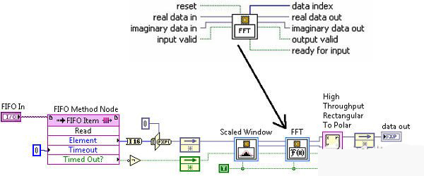
FFT As a fundamental function in DSP, FFT can be used for many test applications. FPGAs have this capability to help test applications such as frequency-domain triggering, data compression, frequency-based closed-loop control, and image processing. Figure 8 shows how this example implements an FFT using LabVIEW FPGA.
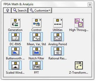
While this article mentions just a few of the exciting digital signal processing capabilities of FPGAs, there are many other capabilities available on FPGAs that can be used in test applications. Many open FPGAs have this type of processing, and Figure 9 shows some of the types of processing that NI hardware can do with LabVIEW FPGA


As open FPGAs grow in popularity throughout the test and measurement industry, instruments with fixed functions will be phased out. Instead, the functionality of an instrument will increasingly be defined by software, similar to the way “apps” have revolutionized the mobile device industry. Test applications will no longer be limited by what software capabilities a test vendor can develop, but by the hardware and the imagination of the engineer who uses the instrument.
Haoxinshengic is a pprofessional FPGA and IC chip supplier in China. We have more than 15 years in this field。 If you need chips or other electronic components and other products, please contact us in time. We have an ultra-high cost performance spot chip supply and look forward to cooperating with you.
If you want to know more about FPGA or want to purchase related chip products, please contact our senior technical experts, we will answer relevant questions for you as soon as possible
Our Products