How FPGA Affects the Chip Design Process ?
The use of field programmable gate arrays (FPGAs) can significantly increase the complexity of the design process. These devices can bring higher performance to complex functions and improve overall system performance. This article aims to explore how FPGAs affect the chip design process.
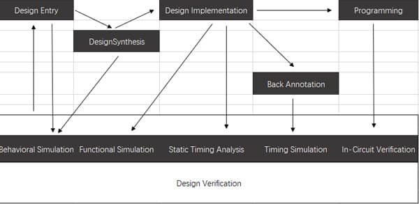
When working with any programmable logic, including FPGAs, there are several steps in the design process. These steps include design entry, design synthesis and design verification (including functional and timing verification, and at various points in the design flow), design implementation, and device programming. The design process for an FPGA presents a variation on this basic process.
The FPGA floorplan determines the structures and functions that should be placed close to each other. It can be used to reduce the amount of delay in the critical path. Floorplanning can be performed when starting the FPGA design process before the first design iteration of design entry (place and route). It can also be used to correct timing issues after problems are identified during various steps of the design verification process. With floorplanning, designers can identify portions of logic that are causing timing problems and correct design input information to reduce routing delays.
Using floorplanning, optimal grouping and connection of FPGA blocks is manually achieved to increase density and performance while reducing latency. The designer uses the floorplan to guide the synthesis tool to determine the structure of the door according to the floorplan. Floorplanning is also an important part of the iterative process of optimizing FPGA performance. It can help improve/optimize timing performance and consistency.
FPGA Design Entry
After floorplanning, design entry is the first step in FPGA design and implementation. It can be done using schematic entry tools or hardware description languages such as Verilog, VHDL or ABEL, which produce register transfer level (RTL) code. Some designers use a mix of schematic input and language-based tools
Schematic entry may take more time, but it also provides designers with more control over the physical placement of the FPGA logic partitioning and interconnect scheme. Using language-based tools can speed up the design entry process and result in lower performance or lower density. Language-based tools have improved to the point where there is often little practical difference between using them and using the more manual schematic entry process.
Using predefined cores for specific functions such as PCI bus interfaces and DMA controllers, or even complete processors, can speed up the design entry process. At the core are predefined functions that are specifically implemented and verified. They can be hard (fixed-function gate-level IP in the FPGA fabric) or soft (implemented in HDL without extensive optimizations to the target architecture). Soft cores are generally easier to use and less expensive, but lower performance and less efficient than hard cores. Using predefined cores reduces design and verification time for commonly used functions.
Design synthesis
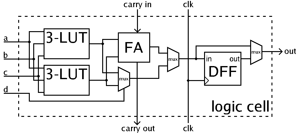
Design synthesis uses instructions from a schematic entry tool or HDL language and generates a gate-level representation or netlist. Synthesis tool generates code bitstream for upload to FPGA.
Boolean algebra is used to formulate FPGA logic and circuit designs. Synthesis tools interpret this logic as look-up tables, flip-flops, RAM blocks, and other elements that make up the FPGA. FPGA synthesis tools serve a similar purpose to software compilers.
C++-based FPGA High-Level Synthesis (HLS) can automatically add pipeline stages and clock constraints to improve performance. Compared to writing code in RTL, HLS can lead to up to 5 times more design efficiency, and the generated C++ code can be 5 to 10 times shorter than RTL code. C++ can also lead to easier reading and fewer bugs because it is expressed at a higher level of abstraction.
HLS verification can be simpler than similar verification using RTL, and using HLS can improve the portability of FPGA designs. Automation of the logic design and synthesis process enables a degree of standardization across various FPGA designs, whether using RTL or HLS.
Design verification
Simulation and design verification are performed throughout the FPGA design flow. In general, three simulation methods are used at different stages of the design process; behavior, structure, and timing.
Originally, behavioral simulation provided a high-level abstraction for RTL description before and during design synthesis. Consider high-level operations, but do not include details on how to implement the design. Perform behavioral simulations using a pre-synthesized HDL description of the FPGA. It runs the fastest, but provides the least design information.
Behavioral simulation verifies syntax and functionality without timing information. This is an important part of the verification process. Identifying errors early will ultimately speed up the design process and reduce the final cost of producing FPGA designs. Once the behavioral aspects of the design are finalized, structural and timing simulation methods can be used to obtain more detailed verification data and optimize the design.
Once the structural and timing simulations are successfully completed, the design is mapped to the netlist. At this stage, multiple simulation iterations can be run. For example, the netlist can be converted to a gate-level description and simulation run to confirm synthesized performance. Finally, the design is ported to the FPGA, and propagation delays can be added, and the simulation rerun to more completely verify the functionality.
Design implementation
After design synthesis, the design is ready to be implemented on the target FPGA. First, the design may need to be converted to a format supported by the design implementation tools provided by the FPGA vendor. This should be fast, even automatic, since most implementation tools can read the netlist format.
These tools translate netlists and perform design rule checking and optimization. Next, divide the design into logic blocks available on the specific FPGA being used. Partitioning is important because good partitioning results in higher routing completion and better FPGA performance.
Once the optimal set of logical blocks has been developed, the implementing software determines the best placement of each block to maximize performance by reducing the number of interconnects required and maximizing available resources. Identify route lengths and possible route track congestion points. In some cases, absolute trace delays are also recognized by the implementing software to meet the design’s defined timing constraints.
The implementation process is similar to the place-and-route procedure used to design a printed circuit board. After successful completion and verification of the implementation, the software generates a binary programming file that can be used to program the FPGA.
In the case of large/complex FPGA designs, implementing software may not be able to successfully complete the design. Implementing software may try several different options and run multiple iterations to reach a fully routed design. It is generally recommended that designers use less than 85% of the available resources on the FPGA to ensure that the design can be implemented to yield a good level of performance.
FPGA programming
Once the programming file is complete, the FPGA can be programmed. The programming method depends on the type of FPGA used. For one-time programmable FPGAs, a device programmer is usually required. In-system programmable FPGAs, such as SRAM-based devices, may not require a dedicated programmer, but still require an intelligent system device to download programming files into the device. This can be done via a microprocessor, microcontroller or via the JTAG test port.
Finally, programming can be done at the FPGA vendor, by a distributor, or the system manufacturer can do the programming at the factory. The system manufacturer’s programming provides the highest level of IP security.
The design flow for an FPGA is similar to the design flow for other programmable devices and custom ICs such as ASICs. Floor planning and the use of pre-designed hardware or software functional cores can help speed up the process.