How to design FPGA automatic loading system scheme
FPGA (Field Programmable Gate Array) is a field programmable gate array. With the development of microelectronics technology, the performance of FPGA has become more and more superior, and the application space has become more and more extensive. FPGA has the feature of supporting repeated programming, but cannot save configuration information after power down. Therefore, after power-on, the user needs to download the designed FPGA configuration file from the external memory to the FPGA to work.
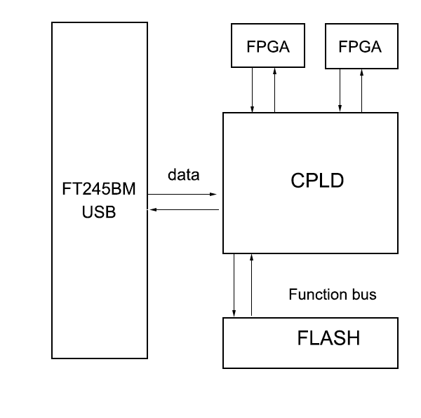
In view of this situation, we propose a FPGA automatic loading system composed of USB chip, FLASH chip and CPLD. The system transmits the configuration file in the PC to the CPLD through the USB chip, and the CPLD writes it into the FLASH chip, and the FLASH chip can store the configuration file for a long time. In this way, after the FPGA is powered on each time, the CPLD will read the configuration file in the FLASH to configure the FPGA. Therefore, the FPGA can automatically obtain the configuration file after each power-on, so that it can work as an independent “chip”, which has strong practicability.
There is also an improvement in the PS mode configuration method. When configuring multiple FPGAs in traditional PS mode, the nCEO of the previous FPGA is usually used to connect the nCE of the next FPGA to enable the next FPGA. In this way, the first FPGA is configured After that, nCEO will enable the next level FPGA to start configuration. In this way, only the first FPGA can be configured first, and there is no free control to configure the next-level FPGA. The CPLD is used to connect two nCEs at the same time. After the previous FPGA is configured, the completion signal is obtained to configure the second FPGA, so that it is not affected by the order of the cascade before and after the FPGA, and the FPGA can be configured freely.
Introduction to system framework and chip
The system consists of CPLD, USB chip and FLASH chip, plus PC part to work with the system. The system framework is shown in Figure 1. In the system, the USB chip connects the PC and the CPLD, and the PC sends commands to the CPLD through the USB to operate the FLASH. First send the erase FLASH command, after erasing or write the configuration file into the FLASH chip. Multiple FPGA configuration files can be stored in the FLASH chip. After power-on or when it needs to be loaded, the CPLD reads the configuration files in the FLASH and configures the FPGA.
Programming FLASH timing
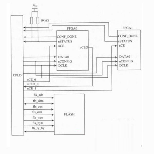
The connection relationship between USB, CPLD and FLASH is shown in Figure 2. The USB sends the commands and configuration files of the PC to the CPLD, and the CPLD controls the FLASH through sequential logic.
The USB chip used in the system is FT245BL from FTDI. After connecting the USB chip to the PC, the USB chip will be automatically recognized as a serial port, and the serial port debugging assistant can be used to send commands or files to it.
Erase and program FLASH operations are as follows:
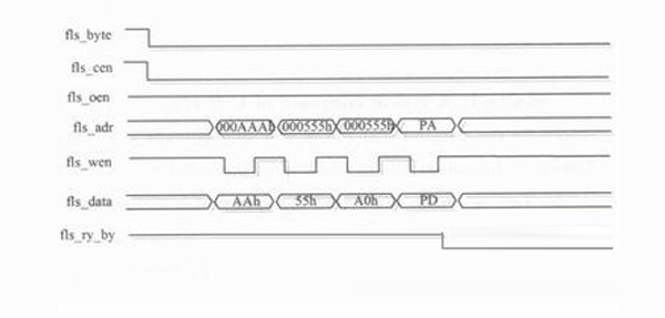
The FLASH chip selects the M29EW series 512MNOR type FLASH of Numonyx. Using asynchronous clock operation, the bit width selection signal corresponding to the fls_byte pin in the timing diagram, pull it low in this system to indicate that the 8-bit wide fls_adr indicates the address, fls_dat indicates the data, fls_cen is the chip enable signal, and fls_oen is the Chip read enable signal, fls_wen is chip write enable signal.
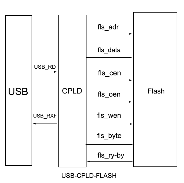
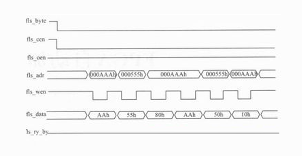
As shown in Figure 3 and Figure 4, when the erase or write operation sequence is performed, the write or erase command can be executed when fls_cen is pulled low and fls_oen is pulled high, the rising edge of fls_wen samples the address, and the falling edge samples the data. fls_ry_by is the busy or idle signal of the chip, and is the only output signal of the FLASH chip, which is used to indicate that an erase or write operation is being performed.
Erase FLASH
Before using the FALSH chip, it needs to be erased, as shown in Figure 3 after the PC sends the erase command to the CPLD through USB. After writing 5 consecutive corresponding addresses and data, the FLASH chip erases the data of the entire chip. As shown in Figure 3, after the execution, the fls_ry_by signal is pulled low to indicate that it has entered the erasing state.
Program FLASH
As shown in Figure 4, when performing the write FLASH operation, firstly, it is necessary to give the data and address corresponding to the three times of writing to the FLASH as the pre-command, and then give the address and data to be written to the FLASH. After receiving the command, the CPLD writes the configuration file of the FPGA into the FLASH according to the timing in the figure.
PS mode automatically loads FPGA
The configuration pins of the FPGA are shown in Figure 5. Configure the FLASH of the FPGA in the PS mode, and the connection relationship between the CPLD and the FPGA is shown in Figure 5
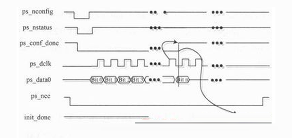
Figure 6 shows the flow chart of loading the FPGA in PS mode. During the loading process, pull ps_nce low and pull ps_nconfig low for at least 40μs and then pull it high. Normally, this operation will cause ps_nstatus to generate a low-to-high pulse signal and make ps_conf_done change from high to low. Give ps_dclk and ps_data0 to configure the FPGA immediately at the moment when ps_nstatus generates a rising edge, wherein the ps_data0 signal is realized by reading the data in the FLASH chip.
The FPGA will automatically recognize the end of the file in the process of receiving the configuration file. After the configuration is completed, the ps_conf_done signal will be pulled high to indicate the end of the configuration. During the configuration process, the init_done will change from high to low. After at least 18μs, the init_done signal will be pulled high to indicate completion. Initialize, then enter user mode.
The conventional method uses nCONFIG, nSTATUTS, CONF_DONE multiplexing, and the nCE of the previous level of FPGA is connected to the nCEO of the next level of FPGA, so the loading order is fixed, and each loading can only load the first FPGA first, to be loaded Only then can the second FPGA be loaded. The difference from the conventional configuration method is that the FPGA that needs to be configured is selected by enabling nCE, and the corresponding configuration file and the timing of the signal ps_conf_done are given to determine whether the configuration is complete, so that the FPGA can be configured freely.
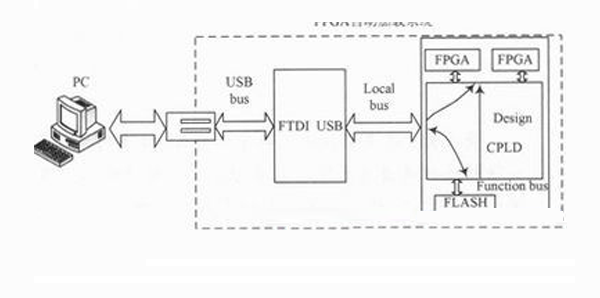
As shown in Figure 7, the platform is automatically loaded by the FPGA. The PC-side configuration file can be written into the FLASH chip through the logic control of the CPLD and the bus of the USB chip. When it is necessary to use the automatic loading function, the CPLD will immediately read out the FPGA configuration file stored in the FLAHS after power-on, and configure the corresponding FPGA in PS mode.
Haoxinshengic is a pprofessional FPGA and IC chip supplier in China. We have more than 15 years in this field。 If you need chips or other electronic components and other products, please contact us in time. We have an ultra-high cost performance spot chip supply and look forward to cooperating with you.
If you want to know more about FPGA or want to purchase related chip products, please contact our senior technical experts, we will answer relevant questions for you as soon as possible
Our Products