How to program FPGAs
FPGA programming involves creating a logic circuit that will execute the requested algorithm and describe it using a hardware description language. Therefore, the building blocks of this algorithm are not variables, conditions, and a set of operations to perform, but logic gates, adders, registers, and multiplexers. The described circuit will eventually be compiled into logic modules – the building blocks of the FPGA.
1. Building blocks of logic circuits
All computers are electronic machines that use Boolean logic to perform operations. In Boolean logic, variables can only be assigned two values: true and false. FPGA logic blocks are designed to perform arbitrary Boolean operations with a specific number of inputs and outputs.
Combinatorial logic implements arbitrary truth tables and basic operations on multi-bit Boolean variables. The multiplexer selects one of the input paths based on the condition. Ripple carry adders enable fast addition and subtraction of variables of arbitrary length without using combinational logic. Finally, registers are used to store boolean values.
2 . Languages used in FPGA programming
Hardware description languages are used to assemble these FPGA building blocks into circuits that will perform specific tasks, making programming different from typical high-level languages. The two most popular hardware description languages are VHDL and Verilog. The syntax of VHDL is similar to Pascal. However, Verilog is similar to C.
A . Writing a Counter in VHDL
To demonstrate how to use a hardware description language, we will write a simple but ubiquitous hardware module – a counter. Our language of choice will be VHDL. Despite being a complex and somewhat outdated language with certain flaws, the simple hardware design in VHDL is self-explanatory.
VHDL files start with the keywords library and use. First, we define the library we are going to use in the code below. Its C counterpart is the include section.
					library ieee;
use ieee.std_logic_1164.all;
use ieee.numeric_std.all;
Library std_logic_1164 contains definitions for std_logic and std_logic_vector. These two model logic states are related to single- and multi-bit signals, respectively. In addition to zeros and ones, these types also contain special values that match logical uncertainties and uninitialized values for hardware design simulation. The library numeric_std contains signed and unsigned data types and conversion functions to and from std_logic types. In our example, the unsigned type will be used in addition to std_logic and std_logic_vector.
					entity universal_counter is
    generic (
        BIT_WIDTH : integer := 8
    );
    port (
        clk    : in  std_logic;
        rst    : in  std_logic;
     load   : in  std_logic;
        enable : in  std_logic;
        input  : in  std_logic_vector((BIT_WIDTH-1) downto 0);
        output : out std_logic_vector((BIT_WIDTH-1) downto 0)
    );
end universal_counter;
The second part of the code is the entity declaration. We declare universal_counter as a design element with generics and ports. Generics in VHDL allow us to synthesize the same element in different variants. In this case, multiple counters may have different widths, and the compiler assumes a default value of 8 when no generic is passed. Ports in VHDL define the inputs and outputs of entities. In the case of universal_counter, we have five input ports and one output. Ports include: clock clk, reset rst, load to assign the new value in the input to the counter, enable the counter to work, and finally output the value of the counter.
					architecture rtl of universal_counter is
    signal value_r, value_next : unsigned((BIT_WIDTH-1) downto 0);
begin
The circuit design of the entity is specified in the Architecture section. In VHDL, a single circuit may have multiple architectures. This is because different goals require different design approaches. For example, the architecture of the FPGA entity must utilize all features of the target FPGA device, such as logic blocks, memory, and DSP blocks (if available). On the other hand, the architecture of an ASIC circuit must be self-contained and must avoid resource-intensive components such as memory and multipliers.
In our example, we specified the register transfer level architecture. The register transfer stage means mapping a circuit with both sequential elements (such as registers) and combinatorial elements (such as logic). The architecture contains two signals of unsigned type. Signals are hardware components to which values can be assigned in an architecture. In our example, signals are used to implement flip-flops. Signal value_r stores the current value of the output, and signal value_next stores the next value, which is derived using combinatorial logic.
All statements defined within the schema are run in parallel. A schema definition begins with the keyword begin.
					process(clk, rst)
    begin
        if rst = '1' then
            value_r <= (others => '0');
        elsif rising_edge(clk) then
            value_r <= value_next;
        end if;
    end process;
Process is a special, event-driven statement in VHDL. Whenever the values in the sensitivity list (in our case clk and rst) change, the instructions in the flow statement are run sequentially. Additionally, VHDL processes can define their own variables for use within the process. In our example, we assign zero to the signal value_r if a reset is triggered, and a derived value every clock cycle otherwise.
					 value_next <= unsigned(input) when load = '1' else
                  value_r + 1     when enable = '1' else
                  value_r;
This assignment is used to derive value_next from a known logical value within the schema. Since the signal is of unsigned type, the input must be converted before use, but don’t worry, this and many other cases will be resolved by the compiler and will be implemented using combinational logic: multiplexers and adders.
					output <= std_logic_vector(value_r);
end rtl;
The last statement assigns the trigger’s value to the output. VHDL architecture is completed with the keyword end.
B . Simulate a counter with VHDL
To simulate a counter, we must define a stimulus. Stimuli are virtual entities that generate input signals for a design. More complex stimuli not only generate input signals, but also compare the output of the hardware design with the output generated by the reference model to ensure the design is working as expected.
Like the universal_counter entity, the incentive source file begins with a library and entity declaration.
					library ieee;
use ieee.std_logic_1164.all;
use ieee.numeric_std.all;
entity tb_counter is
end entity;
Since we don’t want to provide or receive any data, the entity part can be empty. For the same reason, the schema part of the file is more complex than the previous one.
					architecture tb of tb_counter is
    component universal_counter is
        generic (
            BIT_WIDTH : integer := 8
        );
        port (
            clk    : in  std_logic;
            rst    : in  std_logic;
            load   : in  std_logic;
            enable : in  std_logic;
            input  : in  std_logic_vector((BIT_WIDTH-1) downto 0);
            output : out std_logic_vector((BIT_WIDTH-1) downto 0)
        );
    end component;
    signal s_clk    : std_logic;
    signal s_rst    : std_logic;
    signal s_load   : std_logic;
    signal s_enable : std_logic;
    signal s_input  : std_logic_vector(3 downto 0);
    signal s_output : std_logic_vector(3 downto 0);
begin
The schema definition contains a component declaration similar to the universal_counter entity. Actually, it will resolve it and use the previously defined entity. Also, we need signals to communicate with components. In the next section, we will implement a 4-bit counter. Therefore, both the s_input and s_output signals have a width of 4 bits.
					DUT: universal_counter generic map (
        4
    ) port map (
        clk => s_clk,
        rst => s_rst,
     load => s_load,
        enable => s_enable,
        input => s_input,
        output => s_output
    );
The mapping section connects the wires of the component with the signals defined in the architecture section. Since we’re only using one generic, to specify that the counter is 4 bits, we don’t need to specify the name of the generic. Instead, when mapping ports, you must manually connect each port to a matching signal. The DUT name specified at the beginning of the component map is the name of the component. It allows us to access specific components in the mock.
					  CLK_GEN: process(s_clk)
    begin
        if s_clk = 'U' then
            s_clk <= '1';
        else
            s_clk <= not s_clk after 5 ns;
        end if;
    end process;
To generate the clock, we need to take advantage of the event-driven nature of the process statement. In process CLK_GEN, each signal is set to uninitialized (value U in std_logic) at the start of the simulation. So generate an event on s_clk that triggers the process of first setting the signal, then cancelling it after half a clock cycle (let’s say 10 nanoseconds).
					 STIMULUS: process
    begin
        s_rst <= '1';
        s_load <= '0';
        s_enable <= '0';
        s_input <= (others => '1');
        wait for 10 ns;
        s_rst <= '0';
        s_load <= '1';
        wait for 10 ns;
        s_load <= '0';
        s_enable <= '1';
        wait;
    end process;
end;
When using a procedural statement without a sensitive list, the instructions are run once in sequence. First, we set the reset signal to initialize the component. Furthermore, we explicitly set all values of the input signal. On the next clock cycle, we disable the reset signal and load the input value of the counter previously set to the maximum value. Finally, we set the enable signal. Using HDL simulation tools, we can observe the behavior of entities.
3 . Synthetic Counter
Synthesis is the process of mapping the described hardware to the logic modules described in Chapter 1. If we want to use a specific board, we only need to specify the target device and the required pinouts to perform synthesis of the presented counters. No other entity is required.
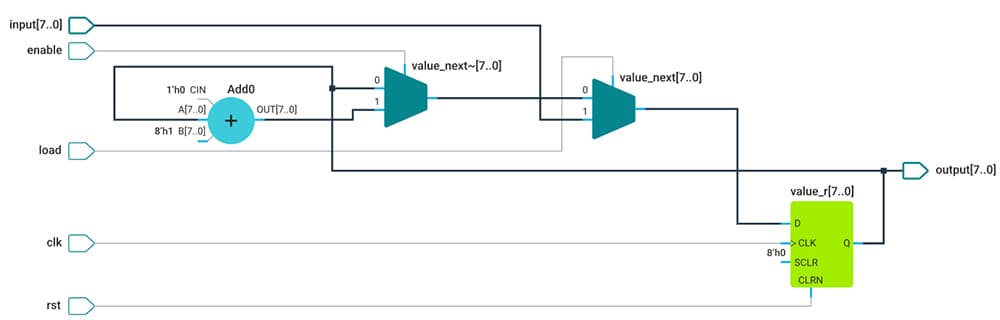
Netlist – A scheme showing how the FPGA compiler understands the circuit in a hardware description language is shown below. As we can see, this design requires a multi-bit adder, two multiplexers, and a registry.
Haoxinshengic is a pprofessional FPGA and IC chip supplier in China. We have more than 15 years in this field。 If you need chips or other electronic components and other products, please contact us in time. We have an ultra-high cost performance spot chip supply and look forward to cooperating with you.