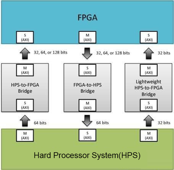
Interconnection structure between FPGA and HPS
There are three main ways to interconnect the structure between programmable logic (FPGA) and hard core processor (HPS). In this article, we will analyze how these three interconnect structures map to each other and handle communication, and which components need to manage timing and have access rights.

AXI Bridge
In order to realize the communication interface between HPS and FPGA, the AXI bridge protocol is derived. The AXI bridge protocol handles bandwidth adaptation and clock control, and supports bidirectional logic and data interaction between HPS and FPGA.

HPS to FPGA
There are two types of HPS to FPGA: high throughput and low throughput. High-throughput data bandwidth can be 32-bit, 64-bit or 128-bit, it is specially designed for high-bandwidth data transmission, HPS as the main, in the L3 layer.
A lightweight (or low throughput) channel is limited to 32 bits, however it is optimized for the lowest latency. Its main function is to pass control and status registers to the FPGA. In addition, it also divides the communication channel from HPS to FPGA. The specific analog description is shown in Figure 1. There are two channels from HPS to FPGA: the first is the 32-bit data channel with higher speed limit, the other is Many channels are designed to support higher bandwidth and more data transfer at the same time.
FPGA to HPS
The third channel of Fig. 1 is to realize the data transmission from FPGA to HPS. The purpose of its design is to access the HP slave interface or wait for the input of data at the HPS program end. It can be configured for 32-bit, 64-bit or 128-bit data bandwidth and is controlled by the HPS L3 master switching clock.
To tie these communication channels together, I started looking through the Intel Developer Community’s Gold Hardware Reference Design Guide (GHRD), which provides some examples of how to set up an AXI bridge channel between the FPGA and the HPS, with which I Really appreciate the powerful function of “Configuration Wizard”, only need to click six mouse clicks to complete the configuration of three communication channels, and can also configure memory allocation. The HPS bridge is mapped to on-chip memory to achieve as little latency as possible. The FPGA part is mapped to the slave memory address, and the data is written to the memory when there is data.
So what does this mean? Communication channels and different transport layers also don’t have many opportunities for some experienced with small, low-power MCUs. Nonetheless, those developers who are used to ARM MCU programming may be familiar with these communication channels (Bridge).
These communication channels are actually a series of control registers and memory maps that are accessed at very high speeds, which is very useful for multi-threaded, multi-core systems that require high-speed, multi-purpose data transfers. Of course this idea of interconnection is very common among MCU enthusiasts.
Using internal interconnect communication channels to divide tasks is very familiar, but accessing them as memory or RAM is somewhat novel. In simple terms, the L3 layer is designed to implement the communication mechanism from FPGA to HPS, and supports data transmission between different processor cores. It opens up the FPGA resources to perform some tasks that the HPS needs to complete, otherwise the HPS will be greatly hindered, and ultimately improve the system performance as a whole.
Haoxinshengic is a pprofessional FPGA and IC chip supplier in China. We have more than 15 years in this field。 If you need chips or other electronic components and other products, please contact us in time. We have an ultra-high cost performance spot chip supply and look forward to cooperating with you.
If you want to know more about FPGA or want to purchase related chip products, please contact our senior technical experts, we will answer relevant questions for you as soon as possible
Our Products