Xilinx, Intel and Lattice three FPGA comparison
In recent years, the FPGA market has been booming, and more and more chip manufacturers have launched different types of FPGAs. Faced with so many different FPGAs, do you know how to choose the most suitable FPGA product? In this article, we will briefly examine three recently announced FPGAs from Xilinx, Intel, and LatTIce.
Each of these FPGAs focuses on a different aspect of improving performance: The Xilinx VU57P attempts to bypass memory bandwidth challenges in demanding applications. Intel StraTIx 10 NX FPGA integrates AI-optimized DSP blocks to help realize large AI models with low latency. Moreover, Lattice Nexus FPGAs attempt to redefine low power, small form factor FPGAs.
Xilinx VU57P FPGA—High Bandwidth Memory
Computational bandwidth has grown exponentially in many application domains over the past decade. For example, the number of DSP slices Xilinx FPGAs provide for machine learning applications has increased from about 2,000 slices in the largest Virtex 6 FPGAs to about 12,000 slices in modern Virtex UltraScale+ devices. Similar trends have been observed in other application domains such as web technologies and video applications as shown below.
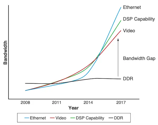
The graph above shows that DDR technology has seen only a slight increase in memory bandwidth over the past decade – roughly a 2x increase from DDR3 to DDR4. (It’s worth noting that the leap from DDR4 to DDR5 may be even more impactful.)
The bandwidth gap in the graph means that the limited data transfer rate between the FPGA and memory is the bottleneck in these applications. To solve this problem, designers often use multiple DDR chips in parallel to increase memory bandwidth (not necessarily memory capacity). However, this approach becomes unusable at memory bandwidths greater than about 85GB/s due to high power consumption, form factor and cost issues, and PCB design challenges.
Alternatively, an effective solution to the memory bandwidth problem is a type of DRAM-based memory known as High Bandwidth Memory (HBM for short). In this case, both DRAM memory and FPGA can be implemented in the same package using silicon stacking technology, as shown in the figure below.

HBM technology allows us to eliminate the relatively long PCB traces connecting the DDR chip to the FPGA. Using an integrated HBM interface with a large number of pins can significantly increase memory bandwidth, with latencies similar to DDR-based technologies.
Xilinx recently released the VU57P FPGA (from the Virtex UltraScale+ family), which integrates 16 G HBM and up to 460GB/s memory bandwidth. The device employs an integrated AXI port switch, allowing us to access any HBM memory location from any memory port.
In addition to the energy-efficient computing capabilities and large memory bandwidth discussed above, the VU57P also offers high-speed interfaces such as 100G Ethernet with RS-FEC, 150G Interlaken, and PCIe Gen4. The new device’s 58G PAM4 transceiver supports connectivity to the latest optical standards. This is useful in different applications such as next-generation firewalls and switches and routers with QoS.
Intel StraTIx 10 NX FPGA — AI-Optimized DSP Block
Many routine applications of digital signal processing (DSP) require high-precision arithmetic. This is why FPGAs usually have DSP blocks with high precision multipliers and adders. For example, the XC7A50T (Xilinx) and 5CGXC4 (Intel) have 120 and 140 18×18 multipliers, respectively.
It turns out that many deep learning applications can be implemented using fewer bits without significantly sacrificing accuracy. A lower precision approximation reduces the amount of computational resources and required memory bandwidth.
Another advantage of reducing the bit width is power savings due to less precise calculations and fewer bits that need to be transferred per memory transaction. In fact, according to the UC Davis researchers, INT8 and even lower-precision calculations can yield acceptable results in many deep learning applications.
The Intel Stratix 10 NX FPGA is the first AI-optimized FPGA from Intel. These devices integrate arithmetic blocks called AI Tensor Blocks, which contain dense arrays of low-precision multipliers. The base precision of these blocks is INT8 and INT4, although they support FP16 and FP12 numeric formats via shared exponent support hardware.
The AI Tensor block (used in Stratix 10 NX FPGA) can increase INT8 throughput by 15 times compared to the DSP block of a standard Intel Stratix 10 FPGA. The high-level block diagram of AI Tensor Block is shown below.
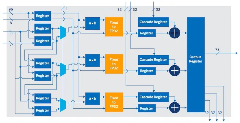
The most notable feature of Intel Stratix 10 NX FPGA is the high computing density provided by AI-optimized computing blocks. However, the new device integrates two other features that further help designers implement their large AI models in a low-latency manner: it supports rich approximate computing memory (integrated HBM) and high-bandwidth networking (up to 57.8 G of PAM4 device).
Lattice Nexus – Low Power, Small Form Factor FPGA
Lattice Semiconductor recently released its Certus-NX FPGA family using 28nm fully depleted silicon-on-insulator (FD-SOI) process technology. FD-SOI was originally developed by Samsung, and it is somewhat similar to the traditional CMOS process. However, it provides programmable biasing for most transistors as shown in the figure below.
Lattice Semiconductor recently announced its Certus-NX FPGA family, which utilizes 28nm fully depleted silicon-on-insulator (FD-SOI) process technology. Originally developed by Samsung, FD-SOI is somewhat similar to conventional CMOS processes; however, it can provide programmable biasing for most transistors, as conceptually illustrated below.
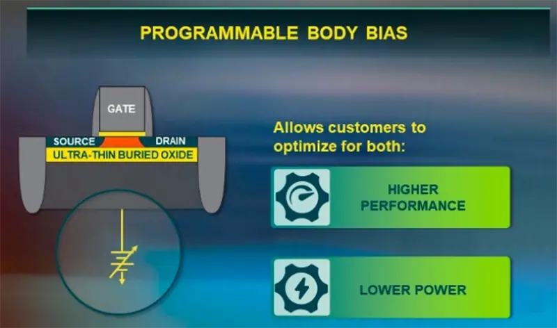
Programmable buck voltage greatly reduces chip area and power consumption. Certus-NX consumes up to four times less power than other FPGAs with similar logic cell counts.
Thanks to the FD-SOI technology, the new devices can be as small as 6mm x 6mm, with up to twice the I/Os per mm2 compared to similar FPGAs. The table below compares the Certus-NX-40 with similar offerings from Intel and Xilinx.
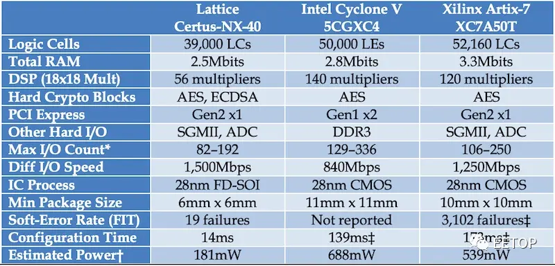
It’s important to note that the new device supports AES for bulk encryption and Elliptic Curve (ECDSA) for authentication. Therefore, it can provide higher security for networked devices. In addition, it has high immunity to soft errors, which makes the device suitable for aerospace applications.
FPGA development trend
By examining these newly announced FPGAs from Xilinx, Intel, and Lattice Semiconductors, we can gain a clearer picture of how FPGAs are evolving—focusing on higher memory bandwidth, AI optimization, low power, and small form factor.
Haoxinshengic is a pprofessional FPGA and IC chip supplier in China. We have more than 15 years in this field。 If you need chips or other electronic components and other products, please contact us in time. We have an ultra-high cost performance spot chip supply and look forward to cooperating with you.
If you want to know more about FPGA or want to purchase related chip products, please contact our senior technical experts, we will answer relevant questions for you as soon as possible
Our Products