[rank_math_breadcrumb]
Lastest News
XILINX Virtex Series
At present, Xilinx has two kinds of FPGA products: Spartan and virtex. The former is mainly for low-cost middle and low-end applications, and is the lowest cost FPGA in the industry at present; The latter is mainly for high-end applications and belongs to the top products in the industry. The difference between these two series is limited to the scale of the chip and the special module. They both adopt the advanced 0.13, 90 or even 65 manufacturing process, and have the same excellent quality.
Virtex series is the high-end product of Xilinx, and also the top FPGA product in the industry. It is with virtex series products that Xilinx wins the market, thus gaining the leading position of FPGA supplier. It can be said that Xilinx leads the field programmable gate array industry with its Virtex-5, virtex-4, virtex-2 pro and virtex-2 series FPGA products. Mainly for telecommunications infrastructure, automotive industry, high-end consumer electronics and other applications. At present, the mainstream chips include vitrex-2, virtex-2 pro, virtex-4 and Virtex-5.
Vitrex-2 series
Vitrex-2 series has excellent platform solutions, which further improves its performance; And the built-in IP core hard core technology can distribute the hard IP core anywhere on the chip, with more resources and higher performance than the virtex series. Its main features are as follows: 0.15/0.12 process is adopted; The nuclear voltage is 1.5V, and the working clock can reach 420MHz; Support more than 20 i/o interface standards; Several hard core multipliers are embedded to improve the processing capacity of DSP; With complete system clock management function, up to 12 DCM modules.
Virtex-2pro series
Based on virtex-2, virtex-2 Pro Series has enhanced the embedded processing function and embedded PowerPC ™ 405 kernel also includes advanced active interconnect technology to solve the challenges faced by high-performance systems. In addition, a high-speed serial transceiver is added to provide a Gigabit Ethernet solution. Its main features are as follows: 0.13 process is adopted; The nuclear voltage is 1.5V, and the working clock can reach 420MHz; Support more than 20 i/o interface standards; Two powerpcs with high-performance RISC technology and frequency up to 400MHz are added ™ Processor; Add multiple 3.125gbps rocket serial transceivers; Several hard core multipliers are embedded to improve the processing capacity of DSP; With complete system clock management function, up to 12 DCM modules.
Virtex-4 series
Virtex-4 device integrates up to 200000 logic units, up to 500 MHz performance and unparalleled system characteristics. Virtex-4 product is based on the new advanced silicon wafer assembly module (asmbl) architecture, and provides a multi platform mode (LX, SX, FX), so that designers can choose different development platforms according to their needs; The logic density is high, and the clock frequency can reach 500MHz; It has DCM module, pmcd phase matching clock divider and on-chip differential clock network; 500MHz smartram technology with integrated FIFO control logic is adopted, and each i/o is integrated with 1 Gbps i/o of chipsync source synchronization technology and Xtreme DSP logic chip. Its main features are as follows: it adopts 90 technology and integrates up to 200000 logic units; System clock 500MHz; 500MHz smart RAM Technology with integrated FIFO control logic is adopted; It has DCM module, pmcd phase matching clock divider and on-chip differential clock network; Each i/o is integrated with 1Gbps i/o of chipsync source synchronization technology; It has super signal processing ability, integrates hundreds of XtremeDSP slice, and the maximum processing rate of a single chip is. Virtex-4 LX platform FPGA is characterized by a density of up to 200000 logic units. It is one of the FPGA series with the highest logic density in the world, and is suitable for design applications with high demand for logic gates.
Virtex-4 SX platform improves the proportion of DSP, RAM unit and logic unit. It can provide 512 XtremeDSP hard cores at most, and can work at 500MHz. Its maximum processing speed is. It can create more than 40 different functions with it, and can realize larger DSP modules in multiple combinations. Compared with virtex-2 Pro Series, it also greatly reduces the cost and power consumption, and has extremely low DSP cost. The FPGA of SX platform is very suitable for high-speed and real-time digital signal processing.
Virtex-4 FX platform is embedded with 1-2 32-bit RISC powerpcs ™ The processor provides four 1300 Dhrystone MIPs, 10/100/1000 adaptive Ethernet MAC cores, and the coprocessor controller unit (APU) allows the processor to construct special instructions in FPGA, making the performance of FX devices reach 20 times of the fixed instruction mode; In addition, it also includes 24 rocket i/o serial high-speed transceivers, which support common high-speed transmission rates of 0.6gbps, 1.25 Gbps, 2.5 Gbps, 3.125 Gbps, 4 Gbps, 6.25 Gbps, 10 Gbps, etc. FX platform is suitable for complex computing and embedded processing applications.
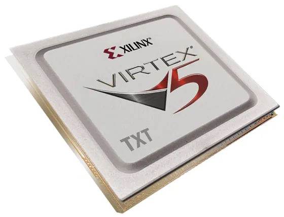
Virtex-5 series
Virtex ®- 5 FPGA is the first 65nm FPGA Series in the world, which is manufactured by using 1.0V, three grid oxide process technology. According to the selected devices, it can provide 330000 logic units, 1200 i/o pins, 48 low-power transceivers and built-in PowerPC ™ 440、PCIe ® Endpoint and Ethernet MAC module. Five series of platforms have been provided, namely LX, LXT, SXT, FXT and TXT. Each platform achieves the best balance in terms of high-performance logic, serial connection function, signal processing and embedded processing performance. For example, LX is optimized for high-performance logic, LXT is optimized for high-performance logic with low-power serial connection function, and SXT is optimized for DSP and memory intensive applications with low-power serial connection function. Virtex-5 FXT is used to realize embedded processing with the highest rate serial connection function, and Virtex-5 TXT can be used to realize ultra-high bandwidth applications, such as bridging, switching and aggregation in wired communication and data communication systems.
It adopts the latest 65 technology and combines low-power IP blocks to reduce dynamic power consumption by 35%; In addition, 65nm tri gate oxide technology is also used to maintain low static power consumption; Using 65nm expressfabric technology, the real 6-input LUT is realized, and the performance is improved by 2 speed levels. The enhanced 36 kbit block RAM with built-in FIFO logic and ECC for building larger arrays has a low-power circuit that can turn off unused memory. Up to 330000 logical units can achieve unparalleled high performance; There are up to 1200 i/o pins, which can realize high bandwidth memory / network interface, 1.25 Gbps LVDS; There are up to 24 low-power transceivers, which can realize 100 Mbps – 3.75 Gbps high-speed serial interface; The nuclear voltage is 1V, and the system clock is 550 MHz; The 550 MHz dsp48e slice has a built-in 25 x 18 Mac, which provides the performance of 352 gmacs, and can realize single precision floating-point operation while reducing the resource utilization by 50%; Use the built-in PCIe endpoint and Ethernet MAC module to improve the area efficiency; The more flexible clock management tile combines a new PLL for precise clock phase control and jitter filtering with a digital clock manager (DCM) for various clock integrations; The second generation spark chevron package is used to improve the signal integrity and reduce the system cost; The device configuration is enhanced to support commercial flash memory, thus reducing the cost.
Virtex-6 FPGA series
Based on the third generation Xilinx asmbl ™ Based on the 40nm manufacturing process of the architecture, virtex-6 FPGA series also has a new generation of development tools and extensive IP library support that has been developed for Virtex-5 FPGA. All these provide strong support for productive development and design transplantation. Compared with 40nm FPGA products provided by competitors, the performance of the new virtex-6 FPGA series is improved by 15% and the power consumption is reduced by 15%. The new device operates on 1.0V core voltage, and there is an optional 0.9V low-power version. These enable system designers to use virtex-6 FPGA in their design, thus supporting the construction of “green” central offices and data centers. This is particularly important for the telecommunications industry, which is expanding its support for Internet video and rich media content.
Virtex-6 FPGA series includes three FPGA platforms optimized for application fields, which provide different combinations of features and functions to better meet the needs of different customer applications:
Virtex-6 LXT FPGA – optimized target applications require high-performance logic, DSP, and serial connectivity based on low-power GTX 6.5gbps serial transceivers.
Virtex-6 SXT FPGA – optimized target applications require ultra-high performance DSP and serial connectivity based on low-power GTX 6.5gbps serial transceivers.
Virtex-6 HXT FPGA – as an optimized communication application, it requires the highest serial connection capability. Up to 64 GTH serial transceivers can provide up to 11.2gbps bandwidth.
Virtex-6 FPGA perfectly combines advanced hardware chip technology, innovative circuit design technology and architecture enhancement. Compared with the previous generation of virtex devices and competitive FPGA products, it has significantly reduced power consumption, higher performance and lower cost. Table 3-15 shows the main technical features of virtex-6fpga series.
